Sunday 16 December 2012

I/O Management


I/O which means input or output is mediated by the OS also known as operating system. I/O resources are shared by multiple programs therefore protection and scheduling is needed. I/O can causes asynchronous interrupts but there are exception for the same mechanism. I/O programming is fiddly as OS provides abstractions to programs.

I/O Commands

I/O devices are managed by I/O controller hardware and data are transferring to and fro device. It also synchronizes operation with software. Command registers will cause device to do something while status registers indicate what the devices is doing and occurrence of errors. As for data register, write simply means  transfer data to a device while read means the other way round.

Technique of I/O

There are 5 types of I/O techniques:
1)      Programmed I/O: The CPU issues a command and wait for I/O operations to be complete. The CPU is faster than the I/O module therefore it is wasteful.
2)      Interrupt Driven I/O: The CPU will issues commands then proceed to its normal work until interrupted by I/O devices on the work completion.
3)      DMA(Direct Memory Access) : In this technique CPU and I/O exchange date without CPU involved.
4)      Memory Mapped I/O: Memory and I/O are treated as memory only which means no signal like IO/M.
5)      Isolated I/O: Address space of memory and I/O is isolated and it uses IO/M signal.
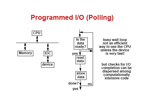
Programmed I/O

Also called polling. It check I/O status register periodically and if device is ready operation will be execute while take action if error occurs. It is common in small or low-performance real-time embedded systems because of its predictable timing and low hardware cost while in other system, CPU time is wasted. The code in the OS for Programmed I/O is more like:
keyboard_wait:               ; for get_ch
      test Keyboard_Status, 80000000h
      jz keyboard_wait
      mov eax, Keyboard_Data
and
   display_wait:                   ; for put_ch
      test Display_Status, 80000000h
      jz display_wait
      mov Display_Data, eax
    This scheme is known as BUSY WAITING, or SPIN WAITING. The little loop is called a SPIN WAIT LOOP.


The problems with Programmed I/O is much time is wasted spin waiting. If it takes 100 instructions to program this, and each instruction takes 20ns to execute, then it takes
   100 * 20nsec = 2000nsec = 2 usec to execute
If a device takes 2msec (=2000usec) to deal with one character, then the percent of time spent waiting
   time waiting / total time = 2000us / 2000us +2us =99.9%
However we will likely have a solution that actually spent less time “doing nothing”.

Interrupt Driven I/O

When a device is ready or an error occurs, controller will interrupts CPU. Interrupt is like an exception but not synchronized to instruction execution and can invoke handler between instructions therefore causes information often identifies the interrupting devices. Priority interrupts are devices needing more urgent attention thus getting higher priority and can interrupt handlers for a lower priority interrupt.

  
Above is the Interrupt Processing and below is the Interrupt Driven I/O Circle.


I/O Data Transfer

For Polling and Interrupt-Driven I/O, CPU transfer data between memory and I/O data registers and its time consuming for high speed devices. Direct Memory Access (DMA) is provided a starting address in memory by the OS and I/O controller transfer to and fro memory autonomously but interrupt upon completion or error.  

Yap Chi Hian B031210334

Saturday 15 December 2012


Direct access memory


 is a feature that allows certain hardware subsystems within the computer to   access system memory independently of the central processing unit(CPU).

-special Purpose processor: DMA controller
           -It has many DMA channels for many peripheral devices.
           -can generate addresses and initiate memory read or write cycles.
           -contains several registers that can be written and read by the CPU.
                     -a memory address register, 
                     -a byte count register, 
                     -one or more control registers.

DMA operation involves loading programs or data files from disk into memory, saving file on disk, and accessing virtual memory pages on any secondary storage medium.
Processor writes the data DMA access data and continuous working.

With DMA, the CPU initiates the transfer, does other operations while the transfer is in progress, and receives an interrupt from the DMA controller when the operation is done. It useful when CPU cannot keep up with the rate of data transfer or needs to perform useful work while waiting for a relatively slow I/O data transfer.

Without DMA, when the CPU is using programmed input/ output. it is typically fully occupied for the entire duration of the read or write operation, and is thus unavailable to perform other work.

DMA controllers are standard components in PC.
Many hardware system using DMA, include graphic card and network card.
Main structure of DMA controller:
                 - Bus buffers
                 - Timing and control

DMA/ VM Interaction

Operating system uses virtual addresses for memory. DMA block may not be contiguous in physical memory. DMA need a controller to translate

If DMA uses physical addresses
             -may need to break transfers into page-sized chunks
             -chain multiple transfers
             -allocate contiguous physical pages for DMA

DMA Transfer
  1. device driver is told to transfer disk data to buffer at address X
  2. device driver tells disk controller to transfer C bytes from disk to buffer at address X
  3. disk controller initiates DMA transfer
  4. disk controller sends each byte to DMA controllers DMA controller transfer bytes to buffer X, increasing memory address and decreasing C until C=0
  5. when C=0, DMA interrupts CPU to signal transfer completion


Input/Output Transfer Mode
  1. Serial
  2. parallel

Serial Transfer

Asynchronous and Synchronous clocking

Asynchronous - no common clock

      data transfer between two independent units requires that control signals be  
     transmitted between the communicating units to indicate the
      time at which data is being transmitted


Two Asynchronous Data Transfer Method

Strobe pulse- A strobe pulse is supplied by one unit to indicate the other unit 
                      when the transfer has to occur

Handshaking- A control signal is accompanied with each data being transmitted to 
                       indicate the presence of data- The receiving unit responds with 
                       another control signal to acknowledge receipt of the data

Synchronous – all derive the timing information from common clock line
                         verification by synchronization pattern

Parallel Transfer

Data Transfer - read sector
                       - write sector

control -Disk seek
Transfer Integrity -transfer parity and data encoding


Kee Hwaai Sziang B031210067


What is Qtspim?

It is newest version of Spim.Spim is a self -contained simulator that runs MIPS 32 programs that emulate MIPS processor.
MIPS processor has 32 general purpose registers, each holding 32 bits.

-  reads and executes assembly language programs written for this processor.
-  provides a simple debugger and minimal set of operating system services.
-  does not execute binary (compiled) programs Spim implements almost the       entire MIPS32 assembler-extended instruction set.

The MIPS architecture has several variants that differ in various ways (e.g., the MIPS64 architecture supports 64-bit integers and addresses), which means that Spim will not run programs for all MIPS processors.


Qt is cross-platform, so the same user interface and same code will run on Windows, Linux, and Mac OS X.


Register display : -list all 32 general purpose registers
                          -display in hex, binary or decimal
                          -initially, content of the register is zero except for the stack pointer

Data display :  contain User Data Segement, User Stack and Kernal Data Segment.
                      Shows the MIPS memory that hold data programmed by the user and
                      usual data that has been pushed into stack.

Text display : 1st column is the addresses of the memory locations of the machine     
                     instruction displayed in hexadecimal on the second column. Whereas, the
                     3rd column code to represent the machine instruction.

Spim Message: show message(errors or not) from the simulator


Kee Hwaai Sziang B031210067


Register Type Instruction Format (R – Type)


This is a group contains all instructions that do not require an immediate value( a value, e.g. 5,-3,etc), target offset, memory address displacement, or memory address to specify an operand. This includes arithmetic and logic with all operands in registers, shift instructions, and register direct jump instructions (jal and jr).

It specify 3 registers(rs,rt,rd), a shift amount field(shamt), and a function field(funct).Opcode for R- type is 000000.


Instruction fields


op
rs
rt
rd
shamt
funct
Operation code
Source register specifier
Target register specifier
Destination register specifier
Shift amount
Function field
         6Bits                         5bits                             5bits                                 5bits                          5bits                   6bits


Instruction coding

-immediate from 0thbit to 5thbit ( 6 bits )
-shamt from 6thbit to 10thbit ( 5 bits )
-rd from 11thbit to 15thbit ( 5 bits )
-rt from 16thbit to 20thbit ( 5 bits )
-rs from 21thbit to 25thbit ( 5 bits )
-op from 26thbit to 31thbit ( 6 bits )


Register type application


a. Non-Jump R -type
               ALU Usage – add rd,rs,rt
b. Jump register
               ALU Usage – jalr rd ,rs
Both:
  1. No update beyond the normal increment.
  2. Source operand fetch: rs and rt.
  3. ALU operation: determined by the function field.
  4. Memory access: none.
  5. Result from ALU write to rd.

eg.add, sub,mult,mul, and ,or,jalr ,jr ,sll...
                   
              add $t0 , $t1 , $t2          # $t0 = $t1 + $t2

              sub $t1 , $t2 , $t3          # $t1 = $t2 + $t3
for unsigned value(positive no only) addu,subu, multu...


              addu    $t1 , $t6 , $t7              #  $t1 = $t6 + $t7 
              subu    $t1 , $t6 , $t7              #  $t1 = $t6 + $t7


mul $t0,$t0, $t1       same as :         mult       $t0,$t1  
                                                         mfhi       $t0

mfhi - move quantity in special register Hi to $t0:   $t1 = Hi 

Why having hi and lo in multiplication and division?
bacause $t3 and $t4 both is 32 bits quantities, they need 2 registers to store it,put their results in MIPS registers Hi. Similar to division , Hi is remaider , Lo is quotient.
                  div $t1,$t2        # t1 / t2
                  mflo $s0        #s0 = quotient
                  mfhi $s1        #s1 = remainder


Kee Hwaai Sziang B03121067

Sunday 9 December 2012

Jump Types Instruction Format


Jump Type Instruction Format

There are three types of instruction format which is Register Type, Immediate Type and Jump Type. However this post will only talk about Jump Type, also known as the J-Type.
J-Type consist of two direct jump instructions : “j” and “jal”. These instruction will require a memory address to specify their operand. J-type instruction use an opcodes of 00001x.
J-type format is as follow :


Addressing Modes
There are five types of addressing modes. There are : Register addressing, Immediate addressing, PC-relative addressing, Base addressing and Psedo-direct addressing. Here we will only explain the last three types.

PC-Relative Addressing
PC-relative addressing is usually used in conditional branches. PC refers to special purpose register, Program Counter that stores the address of next instruction to be fetched.
In PC-relative addressing, the offset value can be an immediate value or an interpreted label value. The effective address is the sum of the Program Counter and offset value in the instruction. The effective address determines the branch target.
PC-relative addressing implements position-independent codes. Only a small offset is adequate for shorter loops.
For example, instruction               beqz $t0, strEnd
                                                   Where; $t0=rs
                                                              100=offset
                                                   Thus; if ($t1==0) goto PC + 4 + (4*2)
In this instruction, beqz is a conditional instruction that branches to label in the code if the content of $t0 is equal to zero. If the current address for branch instruction in execution is 0x4000000C, the effective address will be 40000018. The details of the example will be shown in the following tables.


Address                        
Instruction
Note
40000008
subi $t0,$t0,1
Binary code to beqz $t0, strEnd is 0x110000004, which means 2 instructions from the next instructions.
PC=0x4000000C
PC+4=0x40000010
Add 4*2=0x00000008    
Effective Address=0x40000018
4000000C
beqz $t0,label
40000010
subi $t0,$t0,1
40000014
subi $t0,$t0,1
40000018
strEnd:
subi $t0,$t0,1                  
4000001C
subi $t0,$t0,1


Base Addressing
Is also known as indirect addressing, where a register act as a pointer to an operand located at the memory location whose address is in the register.
The register is called base that may point to a structure or some other collection of date and immediate value is loaded at a constant offset from the beginning of the structure. The offset specifies how far the location of the operand data from the memory location pointed by the base.
The address of the operand is the sum of the offset value and the base value(rs). However, the size of the operand is limited to 16 bits because each MIPS instructions fits into a word.
The offset value is a signed number which is represented in a two’s complement format. Therefore, offset value can also be a negative value.
Consider the following instruction:
lw $t1, 4($t2)
where   $t1=rs
             $t2=base(memory address)
                4=offset value
Thus; $t1= Memory [$t2+4]
The instruction will load register $t1 with the contents of the memory location four words onward from the location pointed by register $t2.
If the offset is negative value; i.e. -4, the operand data is located by 4 bytes back from the location pointed by register $t2.
lw $t1, -4($t2)
$t1= Memory [$t2-4]

Pseudo-Direct Addressing  
Pseudo-direct addressing is specifically used for J-type instructions, “j” and “jal”. The instruction format is 6 bits of opcode and 26 bits for the immediate value(target).
In Pseudo-Direct addressing, the effective address is calculated by taking the upper 4 bits of the Program Counter(PC), concatenated to the 26 bit immediate value, and the lower two bits are 00.
Therefore, the new effective address will always be word-aligned and we can never have a target address of a jump instruction with the two bits anything other than 0 0 and creates a complete 32-bits address. Since the upper 4 bits of the PC are used, this constrains the jump target to anywhere within the current 256 MB block of code(1/16 of the total 4GB address space). To jump anywhere within the 4GB space, the R-type instructions “jr” and “jalr” are used, where the complete 32-bit target address is specified in a register.
NOTE:
word-aligned : This means that an address( unless you use one of the special instructions for loading or storing bytes) must be a multiple of four. An address that isn’t a multiple of four can lead to undesirable results.
               
Consider the following instruction:
 j  label
The implementation of the instruction is best described using the following operation:


Yap Chi Hian B031210334

Input & Output ( function )


Input and Output

I/O devices have three characterized which are
-          Behaviour : input, output, and storage
-          Partner : Human or machine
-          Data rate : bytes/sec, transfers/sec
Input devices – keyboard, mouse, scanner…
Output devices – monitor, printer, speaker…

Function of I/O modules
Input/ Output Module Structure

There are five function on I/O modules which are control & timing, CPU communicating, device communication, data buffering and error detection.

    Control and Timing
It is for control multiple devices all communicating on the same channel.
a.       CPU checks I/O module device status of attached device
b.      I/O module check the status
c.       If ready, CPU requests data transfer
d.      I/O module gets data from device and transfers data to CPU
e.       Variations for output, DMA.
f.       Rate of transmission from device to CPU or vice-versa
I/O System Characteristics
Dependability is important because it is helping for particularly of storage device.
They performance is based on the latency (the time response), throughput (bandwidth of decive), desktops & embedded systems (constant the response time and diversity of devices), and servers (constant the throughput and expandability of devices)

CPU Communication
1.      Processor communication
• Command decoding: CPU sent a command as signals on the control bus for I/O module to work.
• Data: Exchanged between the CPU and I/O module
• Status reporting: Status signals BUSY and READY are reporting to CPU because peripherals are slow
• Address recognition: I/O module will connected a unique address for each peripheral that it controls.

2.      I/O module communication
• Device communication: These are includes commands, status information, and data transfer.
• Data buffering: data comes from main memory in rapid burst and buffered by the I/O module sent to the device at the device’s rate. It is essential function to overcome the speed mismatch other.
• Error detection: For reporting errors to the processor such as bad data.
Dependability
 Service accomplishment will make sure the service delivered as specified. If it is failure of a component and it may lead to system failure, it will send to service interrupt department to deviation again from specified service for restoration. This step will repeat until restoration success it.

Device Communication
It is specific for each input and output device.

Data Buffering
It is define the speed by different device are using. Usually device is oders of magnitude slower, the I/O module will buffer data to keep tie up from CPU's bus with slow read or write.

Error Detection
For disturbing require for checking error to module.

Dependability Measure
It will based on few characteristics to determine it.
1.      Reliability : MTTF, (mean time to failure) to checking the devices.
2.      Service interruption : MTTR,(mean time to repair) to repair the error devices.
3.      Mean time between failures, MTBF = MTTF + MTTR , for repeat the step above until it get successful restore.
4.      Availability : MTTF/ ( MTTF+MTTR )
5.      Improving Availability :  Increase the MTTF, fault avoidance, fault tolenrance and fault forecasting. This all can help to increasing the MTTF value. Besides that, we also can reduce MTTR, the less repair mean less error are find on the devices. SO that we must improved tool and processes for diagnosis and repair to shorter the time.

Bus signals and Synchronization
They are have relation between each other to help to perform more better in the process pass by input and output devices.
·         For data line
They will carry address and data to make it become a multiplexed or separate it nicely to avoid mismatch or error connection.
·         Control line
They will indicate the data type for make sure the transfer are able to detecting that data and synchronize the transaction.
·         Synchronous
Uses a bus clock to cycle the process.
·         Asynchronous
For the control which are lock must getting request/acknowledge for control lines to handshaking.

Interconnecting Components
-          The components are require to interconnecting is between CPU processor, memory, and I/O controller.
-          Bus is sharing the communication channel. The parallel set of wires bus are data and synchronization transfer data. Bus also cause to bottleneck in the process.
-          Performance are limited by physical factors such the wire length, number of connection. These all is the once of the cause to affect the performance.
-          More recent alternative is able to help to increase the high speed serial connection with the switch such network or bookmark function.

Bus types
There are two type which are processor – memory buses and I/O buses.
a.       Processor – memory buses
The wire length is short and high speed. The design between this two component is match to memory organization.
b.      I/O buses
The wire length is longer and it also allow multiple connection happen. Therefore the speed is short compare with processor – memory buses. It is specified by standard for interoperability process. At the end, it also will connect back to processor – memory bus through a bridge to complete it.


ANG KUAN KEE B031210344